 Lighting - LED 1 Lighting - LED 1

The effect of Light Emitting Diodes can be so beautiful, with the emphasis on the plural, without which this work of art would not have been possible. But we will first deal with the singular, i.e. only a
single LED, simplified even much more, with a diode in general.
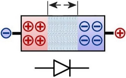
Here is to see the schematic of a typical diode. It consists of a so-called p- and an n-doped layer. For this moment, doped should first be explained as 'contamination'. A barrier layer is drawn between the layers. It becomes
larger at the top when a voltage is applied in the reverse direction.
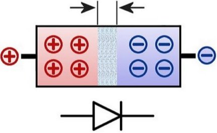
Here the voltage acts in the conducting direction. The positive pole grips the end of the p-doped part and the negative pole grips that of the n-doped part. The switch symbol underneath is therefore basically oriented to the
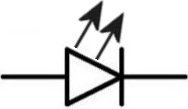
position of the two layers, pointing from the p- to the n-doped one, so to speak. Below you can see what the circuit symbol of a light-emitting diode looks like.
We make it easy for ourselves and only operate a light-emitting diode in the conducting direction. You can imagine that the lack of electrons on the left and the excess of electrons on the right are now canceled. But how is
light created in this process? To explain this, we use the atomic model.
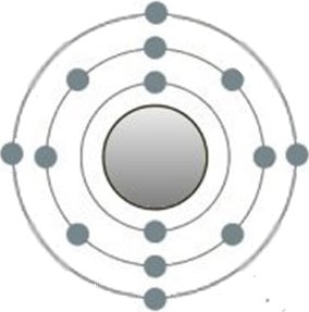
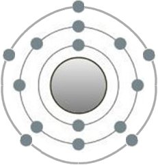
This is the structure of the silicon atom, which belongs to the group of metals. Its 4 electrons on the outermost shell are typical. If more than one silicon atom comes together, the so-called metal bond occurs in place of the
previous one. If more than one silicon atom comes together, the so-called metal bond occurs in place of the previous one. In contrast, the electrons are no longer bound to their respective shells.
This also explains the property of metals as good electrical conductors, namely the presence of free electrons. Now imagine a wafer made of silicon crystals. This is a comparatively larger round plate on which very specific
changes to the structure can be carried out in the finest form.
Perhaps you have already looked into a so-called clean room by video, where even overcoats are common for shoes, for the hair anyway. Here, for example, many microprocessors are produced in the form of wafers, then
divided and connected to the respective connections with very fine, so-called bond wires.
In the case of light-emitting diodes, doping is only done in a targeted manner. Individual silicon atoms are replaced by those with more electrons on the outer shell, such as phosphorus (picture above). An area with an
excess of electrons is created, the n-layer. Conversely, one dopes e.g. with boron (picture below), which has fewer valence electrons than silicon, and receives a p-layer.
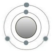
If a voltage is now applied in the direction of conducting, the excess electrons of the phosphorus from the n-layer fill the valence electrons of boron in the p-layer. In doing so, an electron changes proximity to the nucleus,
which, according to Bohr's atomic model, results in the emission of a photon, i.e. a flash of light.
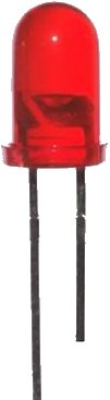
You have probably seen such a light-emitting diode before, so you know how small it is. The longer connection on the left is the anode. More interesting is the cathode, which in this case is worked out in the plastic casing as
a small funnel towards the top. And the piece from the wafer fits exactly into this funnel.
If only a gold bond wire, but it is used here from the part in the funnel to the anode on the left side. It's so fine that you usually don't see it. It must not be too thick either, because otherwise it would take away too much of the
small cone of light upwards.
|